It was a crisp spring morning—March 23, 2023. Inside a modest building complex surrounded by leafy trees in Delhi, cheers erupted in a roar before swelling to a crescendo. A group of military scientists were celebrating a moment they had long worked towards.
Unbeknownst to the rest of the world, Indian military scientists, operating in tandem from Delhi and Hyderabad, had achieved a major breakthrough. They had cracked the code to make gallium nitride (GaN) monolithic microwave integrated circuits (MMICs).

That meant India was no longer dependent on foreign powers for these high-value, cutting-edge chips. Instead, it broke into a select group of six nations—the US, France, Russia, Germany, South Korea and China.
The scene of the celebration was the DRDO’s Solid State Physics Laboratory. The SSPL, which houses a 1,300sqm clean-room (controlled environment, free from contaminants), was designed for sensitive scientific work. The cheering scientists—in sterilised overalls and caps—resembled characters from a sci-fi movie. Ultra-sophisticated, futuristic-looking instruments and equipment bore silent witness to the moment.
MMICs—also called compound semiconductors, because they combine more than one element—are primarily used for specialised applications. They enable superior performance, higher efficiency and faster switching speed than silicon. Compound chips are ideal for extreme environments because of greater chemical inertness and stability at high temperatures or voltages, with very low transmission loss.
Apart from GaN chips, gallium arsenide (GaAs) compound chips are also widely used. While both are superior to silicon for high-frequency data transmission, they serve distinct power requirements. GaAs chips—suited for low to moderate power needs and microwave applications—are cost-effective (commonly used in mobile phones and satellites). GaN chips, with their superior electron mobility, are ideal for high-power and high-temperature uses—they can operate at temperatures of up to 1,000 degrees Celsius.
A GaN chip delivering 30 watts is just 3.5mm x 3mm and can switch power 300 times faster than a silicon chip. It is extensively deployed in military platforms—advanced military drones, missiles, radars, fighter aircraft and naval platforms. The most significant use of compound chips is in sensors that analyse movement, heat, sound, light and changes in pressure, and convert the physical parameters into signals. These signals are used to trigger kinetic action, as well as to monitor and measure conditions.
As warfare undergoes a paradigm shift—from manned to unmanned platforms, and from dependent systems to autonomous ones capable of making split-second decisions—the role of sensors becomes central. With another technological revolution emerging through artificial intelligence and quantum technologies, the importance of compound chips is set to increase even further.
Specific uses include precise navigation, electronic warfare, range finding, night vision and surveillance, camouflage detection, target tracking, missile guidance and imaging through fog, mist and clouds—capabilities that are essential in modern warfare.
While Indian scientists developed GaAs semiconductor technology in the 1990s, GaN chips remained elusive until that Thursday morning in 2023.
Suma Varughese, director general (Micro Electronic Devices and Computational Systems & Cyber Security), DRDO, told THE WEEK that any delay or denial in access to compound semiconductor chips, particularly those based on GaN, could bring several of India’s ambitious defence programmes to a standstill.
Weeks before March 23, GaN MMICs fabricated at the Gallium Arsenide Enabling Technology Centre (GAETEC) in Hyderabad successfully cleared all functionality tests. The GAETEC is also mandated to advance GaAs technology for high-speed and high-power electronic devices.
While the SSPL develops advanced materials and technologies, the GAETEC uses the SSPL’s work to produce MMICs and components. The DRDO and the Indian Space Research Organisation use them in next-generation systems.
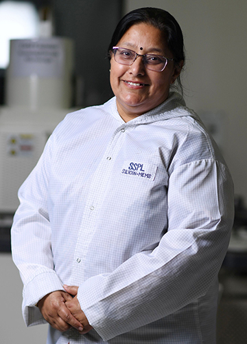
Meena Mishra, director, SSPL, said the news of the breakthrough resulted in a wave of happiness across the entire SSPL/GAETEC team. “Reaching that point involved a long technology development process,” said Mishra, who has been with the SSPL for 35 years. “The teams have worked day and night to make it happen. One cycle of fabrication and testing takes around 80 days and involves hundreds of processes; each has to be executed to its finest detail. The final run is carried out once optimisation of all processes has been finished.” In layman’s language, she added, the dough is now ready; India can use it to make any bread of its choice.
The push to indigenise compound chip production was initiated by, no surprises, former president A.P.J. Abdul Kalam. “Dr Kalam laid the foundation for making indigenous compound semiconductors,” said Mishra. “We successfully supplied to ISRO before moving on to next-generation GaN technology.”
The decisive push with regard to GaN came after foreign entities refused to share technology. Specifically, during negotiations for the purchase of 36 Rafale multirole combat aircraft from France’s Dassault Aviation under a Rs59,000-crore deal.
“In 2016, the order for 36 aircraft was signed as an inter-governmental agreement, mandating a 50 per cent offset clause,” said Mishra. Under the clause, French firms were required to reinvest 50 per cent of the contract value—about Rs30,000 crore—into India through technology transfer, business opportunities and R&D. “India proposed to receive GaN technology under the offset clause, but that was deemed a non-starter because of the strategic and state-of-the-art nature of the technology,” said Mishra. “The circuits were not denied but the technology was.”
In response, the DRDO launched the development of GaN technology. To date, the SSPL and the GAETEC have designed more than 30 chips across frequencies for applications including 5G, radars, satellite communications and electronic warfare.
“Foreign denials and endless delays forced us to innovate,” said Varughese. Strict export controls, including the International Traffic in Arms Regulation, restricted access to compound chip technology. Earlier DRDO programmes such as LSTAR (Long-Range Solid State Active Phase Array Radar, a forerunner to Airborne Early Warning and Control—AEW&C) and AEW&C faced severe difficulties in getting them.
During the development of Netra airborne surveillance platform systems, necessity became the mother of indigenous invention, said Varughese. “We took commercial lower-power GaA chips and pioneered a creative architecture to achieve mission-grade output,” she said. “We also launched indigenous GaN foundry efforts at the SSPL.”
This echoes other episodes in India’s proud history of innovation. When, in 1974, sanctions followed Operation Smiling Buddha, India pursued indigenous solutions.
The 1998 nuclear tests—Operation Shakti—underscored a defiant India’s domestic technological capabilities. The space programme has also become world renowned for its cost-efficient solutions.
However, when it comes to GaN technology, there is still an issue. Reliable GaN fabrication requires ultra-pure precursor gases (99.99999 per cent) and reactors costing hundreds of crores, which India still imports from the US and Europe. “So, we are giving the projects to the academia to be done indigenously,” said Mishra.
Varughese added that depending on foreign sources for strategic electronics was no longer acceptable. “An embargo can arrive overnight,” she said. “Self-reliance in compound semiconductors is not just about savings—it is the bedrock of sovereign capability and the launchpad for tomorrow’s leapfrog technologies.”
India’s sustained investments in space-borne microwave and radar technologies through ISRO’s Space Applications Centre (SAC), Ahmedabad, have strengthened the domestic compound semiconductor ecosystem.
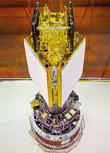
SSPL- and GAETEC-made chips support India’s SBS-3 space-based surveillance programme, which safeguards border and maritime interests. The X-band radar—missile defence and space surveillance—payload alone requires more than 9,000 MMICs, including more than 6,000 produced and screened at GAETEC. X-band components are subject to strict international trade controls.
A senior ISRO official told THE WEEK that GAETEC-fabricated MMICs are now deployed across the spectrum of ISRO missions—large-scale societal applications to strategic radar systems and interplanetary exploration. “GAETEC-manufactured MMICs are used in three RISAT-series C-band radar imaging satellites, each using more than 7,000 chips, of which 5,760 GaAs MMICs were GAETEC-made,” said the official. “It is a major milestone in India’s journey towards semiconductor self-reliance.”
GAETEC’s ability to fabricate, assemble and screen mission-critical MMICs has ensured uninterrupted programme execution and a secure supply chain. The ISRO official added that GAETEC’s MMICs supporting space based communication, navigation, space science and interplanetary missions further demonstrate their technological maturity and reliability for space and deep space operations.
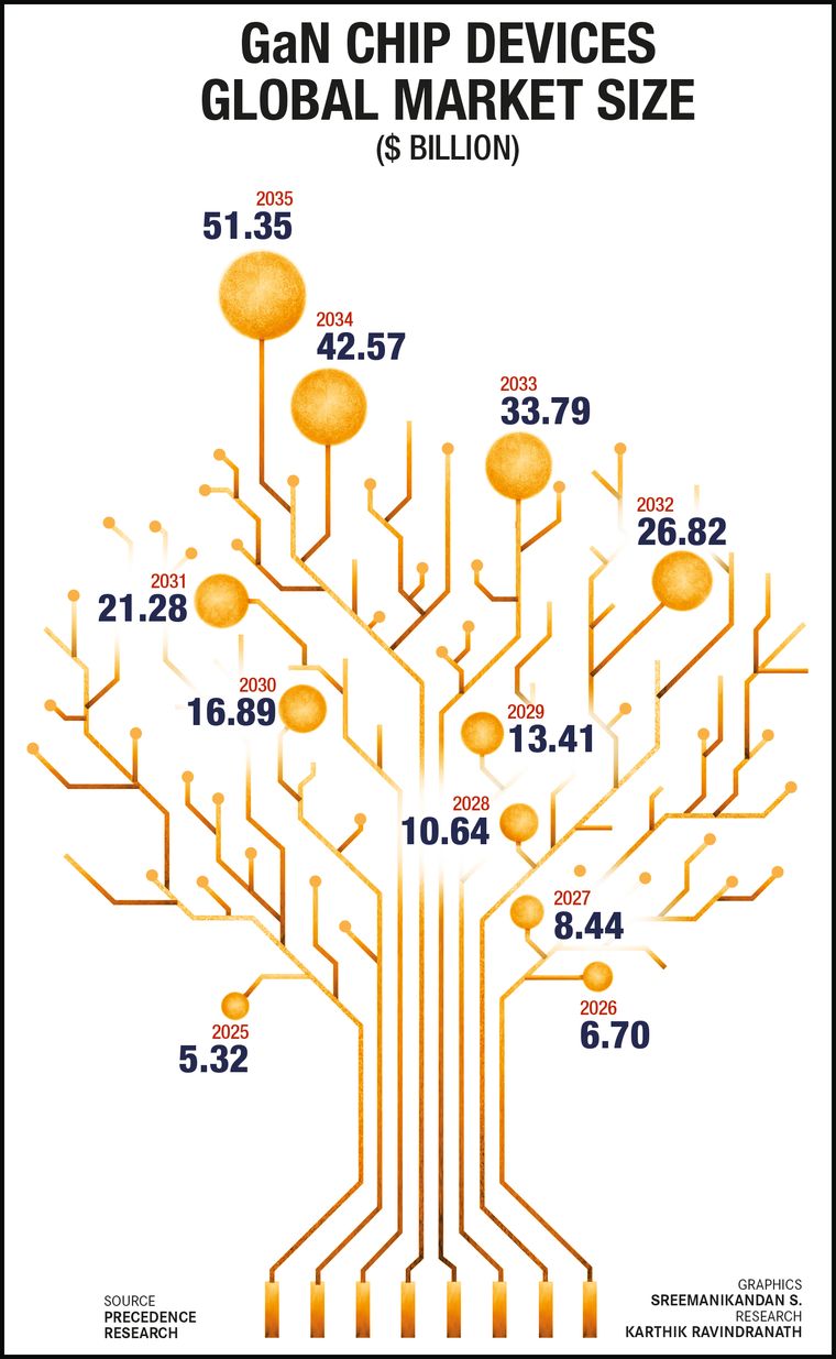
The global GaN semiconductor market was valued at approximately $3.5-$4.1 billion in 2025 and is projected to reach $10-$12 billion by 2030—that is around Rs1 lakh crore based on current exchange rates.
Ankush Bag, associate professor, department of electronics and electrical engineering, IIT Guwahati, said that as more nations establish GaN foundries for local supply, the dependency on other nations will reduce. “This may create regional dominance of GaN technology, and a paradigm shift in geopolitics may be observed,” he said. “Furthermore, the booming commercial GaN market in chargers and 5G will reduce costs and improve manufacturing capabilities.”
As more Indian companies come into the GaN market, he said, there would be a high level of monolithic integration (multiple components on a single chip) to achieve the ultimate goal of maximising performance while minimising size, weight, power consumption and cost.
“The transfer of technology is available from the DRDO at nominal cost for Indian industries,” said Varughese. “The setting of GaN foundries will boost the economy, too.”


